Featured products
-
4WD Mecanum Wheel Smart Car Robot Chassis
Vendor:CokoinoRegular price $33.00 USDRegular priceUnit price per -

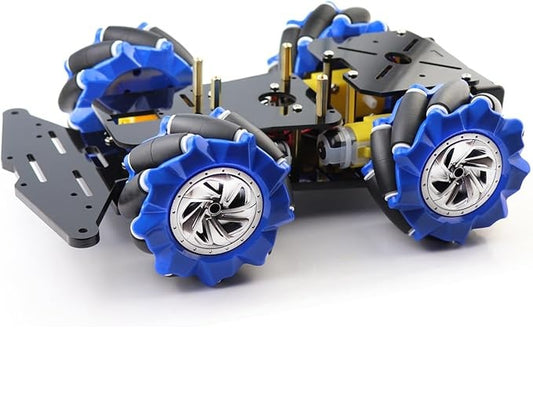
4WD Omni-Directional with Mecanum Wheels Robot Car Kit for Arduino, STEM Education Project Robot Car
Vendor:CokoinoRegular price $54.99 USDRegular priceUnit price per -
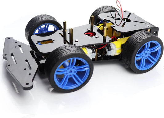
4WD Robot Car chassis Kit
Vendor:CokoinoRegular price $24.99 USDRegular priceUnit price per -
4WD Robot Control Board for Arduino UNO R3 with Buzzer, IR Infrared Receiver and DRV8833 Motor Driver
Vendor:CokoinoRegular price $9.99 USDRegular priceUnit price per


For Arduino
-

For Arduino
Start Kits, Robotics, Boards for Arduino


For Raspberry Pi
-

For Raspberry Pi
Start Kits , Robotics, Boards